Fornet Industries Limited(HK) - A PCB and LED Displays Manufacturer

Our Slogan: Determind to deliver quality, quantity and service for PCB and LED Displays, Fornet is the SMART CHOICE.

Current location: About Fornet Industries Limited(HK) Fornet PCB detail

Visit our online product certification issued by UL

轉到繁體中文版網站

The following are shortcut that you can see what details you what directly.

Process and Production Capabilities in PCB

Process Capability

Item Double Sided Multi-Layers
Base Copper Thickness 18 to 140um 18 to 140um
Board Thickness 0.4 to 3.2mm 0.4 to 2.4mm
CNC Routing Outline Tolerance +/-0.1mm +/-0.1mm
CNC V-groove +/-0.1mm +/-0.1mm
Controlled Impedance 50 to 100ohm +/-10% 50 to 100ohm +/-10%
E-testing Voltage 100 to 300V 100 to 300V
Flammability Rating 94V to 0 94V to 0
Hole Wall Copper Thickness >/=20um >/=20um
Insulation Resistance >/=5M ohm >/=5M ohm
Layer Count 2 4 to 8
Maximum Working Panel Size 550x660mm 550x660mm
Minimum Finished Hole Size 0.2mm 0.2mm
Minimum Line Width or Spacing 0.1/0.1mm 0.1/0.1mm
NPTH Hole Size Tolerance >/=0.05mm >/=0.05mm
Outer Minimum Annual Ring >/=0.1mm >/=0.1mm
Peel Strength 12.0N/cm 12.0N/cm
Punching Outline Tolerance +/-0.127mm +/-0.127mm
Warp and Twist >/=0.75% >/=0.75%

Production Capability

Item Scope
Board Thickness 0.3 to 3.2mm
Bow and Twist </=0.7%(Max)
Copper Thickness 1/2 to 4oz
Flame Rating 94V to 0
Layer 2 to 12
Minimum Annular Ring </=0.125mm
Minimum Finished Hold 0.2mm
Minimum Solder Mask Bridge </=2.5mil
Minimum Trace/Space 0.075/0.075mm
Peel Strength </=12.3n/cm
Punching Outline Tolerance +/-0.1mm
Quality Standards IPC-A-600G, IPC-TM-650, IPC-6012B
Routing Outline Tolerance +/-0.1mm
Working Panel Size 21.5 x 25

Back to top

Quality Commitment of PCB

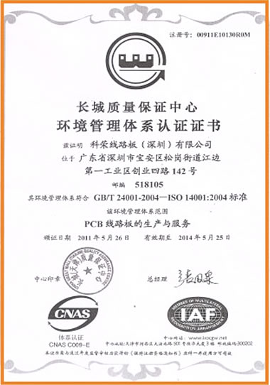
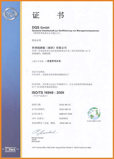
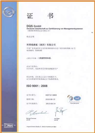
Our factory has been Assessed & Certified by Underwriters Laboratories Inc., (UL) with # E132041 since 1990, Assessed & Certified ISO 9002; 1994 since 1997 and upgraded to ISO in January 2005 Assessed & Certified for TS 16949; 2002 since 2007 and Upgraded to TS 16949: 2009 and ISO9001: 2008.

Our Top Management is committed to make this Facility and ISO 14001:2004 Certified one to support to our customer with all kinds of Rohs finishing surfaces so that we help in creation of “GREEN INDUSTRY” AND A “GREENER WORLD”.

Company Philosophy

Objectives
  • To achieve zero defect
  • To have zero customer claim
Strategies
  • Ensuring that we produce Quality Products
  • Competitive Price
  • On Time Deliveries
  • After-saled Support
  • Effective Communication both Internal and External
  • Keep abreast of the latest Technologies

Back to top

Product Category Show of PCB

ENIG or Gold Plating
PCB ENIG or Gold Plating sample picture
HASL Lead free
PCB HASL lead free sample  picture
Entek(OSP)
Entek(OSP) sample  picture

Back to top

Equipments that we used in PCB

Major Equipment that we own

  • Hitachi Drilling Machine
  • Solder Mask Developing Machine
  • Automated Production Line/Single Line
  • OSP Line
  • TDR Impedance Test
  • Flying Probe Tester

Main Equipment list that we used in PCB

  • Drilling
    Cutting Machine
    1 unit
    Drilling Machine
    6 units
    Sorubbing Machine
    6 units
  • Electronic Plating
    Alkaline Etching Line
    1 unit
    Pattern Plating Line 1
    1 unit
    Pattern Plating Line 2
    1 unit
    PTH Line
    1 unit
  • Outer D/F
    Auto Exposure Machine
    4 units
    Developing Ethching Line
    1 unit
    Laminator
    1 unit
  • Solder Mask
    Solder Mask Exposure Machine
    4 units
    Solder Mask Printing Machine
    4 units
    Solder Mask Developing Machine
    1 unit
  • Profilling
    CNC Machine
    4 units
    Legend Print Machine
    2 units
    Punch Machine
    2 units
    V-cut Machine
    3 units
  • ET
    ET Machine
    4 units
    FG Cleaning Line
    1 unit
    Flying Probe Machine
    2 units
  • Package
    OSP Line
    1 unit
    Vacuum Packager
    1 unit
  • ME Department
    Film Developing Machine
    1 unit
    Vertical Oven
    1 unit
  • One Layer Production Line
    Automatic Production Line For one Layer Board
    1 unit

Back to top

Inner and Outer Layer Process Flow Sequence of PCB

Inner Layer Process Flow Sequence

  1. Board cutting
  2. First time baking
  3. Inner layer imaging
  4. Inner inspection
  5. SES line
  6. AOI
  7. Brown oxide
  8. Lay up
  9. Pressing
  10. Targe hold drilling
  11. Edge routing

Outer Layer Process Flow Sequence

  1. Board cutting
  2. Baking
  3. Drilling
  4. Drilling inspection
  5. Deburring
  6. PTH
  7. Panel Plating
  8. Outer imaging
  9. Outer inspection
  10. Pattern plating
  11. Etching
  12. Tin stripping
  13. Wet film solder mask
  14. Legend
  15. ENIG or Gold plating or HASL
  16. Rout and Punch
  17. V-cut
  18. E-testing
  19. Final inspection
  20. Final audit
  21. OSP + Online inspection
  22. Packing

Back to Top

Major Material Source

As the table below, both of our PCBs made by following materials and come from these suppliers and their Orgins

Type Supplier Origin
Copper Foil Elite Taiwan
Dry Film Hitachi Japan
Laminate(CEM-3) Matsuhita Japan
Laminate(FR-4) Kingboard Hong Kong
Shenyi HuaZheng
Huazheng China
OSP(F2) Shikoku Japan
Prepreg Kingboard Hong Kong
Shen Yi Hong Kong
Solder Mask Taiyo Japan
Green Cure China
Tamura Japan

Back to Top

Product Proportion

The following table showes the proportion of our product produce

Sector Percentage
Automobile 20
Communication 10
Consumer product 20
Home appliance 10
Power(UPS, Invetors and Energe meter) 20
Other 20

Yearly Sales Amount Table

Year Sales Amount(RMB)
1998 17 Million
1999 15 Million
2000 18 Million
2001 20 Million
2002 22 Million
2003 22 Million
2004 18 Million
2005 24 Million
2006 24 Million
2007 30 Million
2008 25 Million
2009 30 Million
2010 35 Million
2011 40 Million
2012 46 Million
2013 55 Million
2014 54 Million

Back to Top

Partner that we currently cooperate with(by alphabetical order of country)

  • China
    • Zowee Limited
    • TPV Limited
  • India
    • Anand Industries Enterprised
    • Dixon Technologies Private Limited
    • Elymer Internation Private Limited
    • Larsen and Toubro Limited
    • Luminous Power Technologies Private Limited
    • Spark Minda, Ashok Minda Group
    • Moser Baer India Limited
    • MRO-TEK Limited
    • Pricol Limited - Coimbatore
    • Secure Meters Limited - Udaipure
    • SGS Tekniks Manufacturing Private Limited
  • Italy
    • COFI s.r.l Limited
  • Singapore
    • Flextronic Technology - Malaysia
    • Flextrnoic Techonology - China Doumen
  • Turkey
    • Vestel Group Limited
  • Ukraine
    • VTN-Ltd (Automotive Supplier)
  • USA
    • APC by schneider electric

Back to Top

Certificates that we own

  • China Great Wall Quality Assurance Center - GB/T 24001-2004 ISO 1400I:2004 Standard
  • DQS GmbH - ISO/TS 16949:2009
  • DQS GmbH - ISO 9001:2008

Back to Top